- 您现在的位置:买卖IC网 > Sheet目录336 > LC4064ZC-EV (Lattice Semiconductor Corporation)BOARD EVAL FOR ISPMACH 4064ZC
�� �
�
�Lattice� Semiconductor�
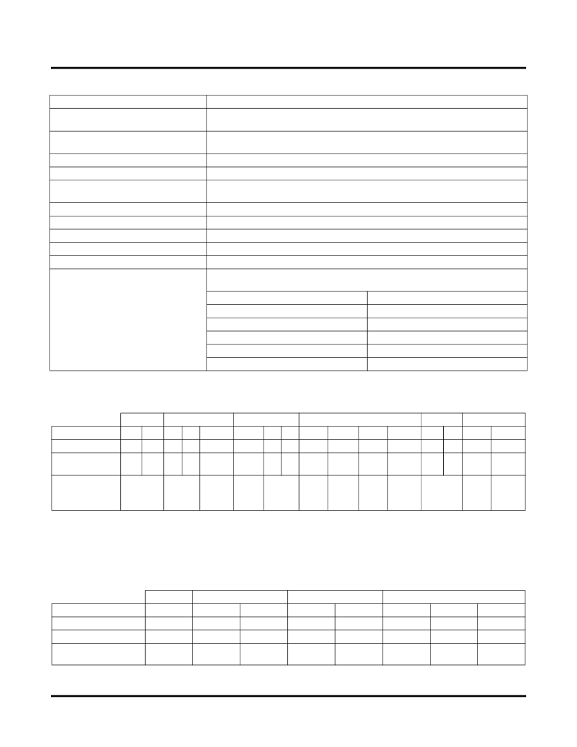
�Signal� Descriptions�
�Signal� Names�
�TMS�
�TCK�
�TDI�
�TDO�
�GOE0/IO,� GOE1/IO�
�GND�
�NC�
�V� CC�
�CLK0/I,� CLK1/I,� CLK2/I,� CLK3/I�
�V� CCO0� ,� V� CCO1�
�ispMACH� 4000V/B/C/Z� Family� Data� Sheet�
�Description�
�Input� –� This� pin� is� the� IEEE� 1149.1� Test� Mode� Select� input,� which� is� used� to� control�
�the� state� machine.�
�Input� –� This� pin� is� the� IEEE� 1149.1� Test� Clock� input� pin,� used� to� clock� through� the�
�state� machine.�
�Input� –� This� pin� is� the� IEEE� 1149.1� Test� Data� In� pin,� used� to� load� data.�
�Output� –� This� pin� is� the� IEEE� 1149.1� Test� Data� Out� pin� used� to� shift� data� out.�
�These� pins� are� configured� to� be� either� Global� Output� Enable� Input� or� as� general� I/O�
�pins.�
�Ground�
�Not� Connected�
�The� power� supply� pins� for� logic� core� and� JTAG� port.�
�These� pins� are� configured� to� be� either� CLK� input� or� as� an� input.�
�The� power� supply� pins� for� each� I/O� bank.�
�Input/Output� 1� –� These� are� the� general� purpose� I/O� used� by� the� logic� array.� y� is� GLB�
�reference� (alpha)� and� z� is� macrocell� reference� (numeric).� z:� 0-15.�
�ispMACH� 4032�
�ispMACH� 4064�
�y:� A-B�
�y:� A-D�
�yzz�
�ispMACH� 4128�
�ispMACH� 4256�
�ispMACH� 4384�
�ispMACH� 4512�
�y:� A-H�
�y:� A-P�
�y:� A-P,� AX-HX�
�y:� A-P,� AX-PX�
�1.� In� some� packages,� certain� I/Os� are� only� available� for� use� as� inputs.� See� the� signal� connections� table� for� details.�
�ispMACH� 4000V/B/C� ORP� Reference� Table�
�4032V/B/C�
�4064V/B/C�
�4128V/B/C�
�4256V/B/C�
�4384V/B/C�
�4512V/B/C�
�Number� of� I/Os�
�30�
�1�
�32�
�30�
�2�
�32�
�64�
�64�
�92�
�3�
�96�
�64�
�96�
�4�
�128�
�160�
�128�
�192�
�128�
�208�
�Number� of� GLBs�
�Number� of� I/Os� /�
�GLB�
�2�
�16�
�2�
�16�
�4�
�8�
�4�
�8�
�4�
�16�
�8�
�8�
�8�
�12�
�8�
�12�
�16�
�4�
�16�
�8�
�16�
�8�
�16�
�10�
�16�
�8�
�16�
�8�
�16�
�8�
�16�
�Mixture�
�of� 8� &� 4� 5�
�Reference� ORP�
�16� I/Os� /�
�8� I/Os� /�
�16� I/Os� /� 8� I/Os� /� 12� I/Os� /� 4� I/Os� /� 8� I/Os� /� 8� I/Os� /� 10� I/Os� /�
�8� I/Os� /�
�8� I/Os� /�
�8� I/Os� /�
�GLB�
�Table�
�GLB�
�GLB�
�GLB�
�GLB�
�GLB�
�GLB�
�GLB�
�GLB�
�GLB�
�GLB�
�GLB�
�4� I/Os� /�
�GLB�
�1.�
�2.�
�3.�
�4.�
�5.�
�32-macrocell� device,� 44� TQFP:� 2� GLBs� have� 15� out� of� 16� I/Os� bonded� out.�
�64-macrocells� device,� 44� TQFP:� 2� GLBs� have� 7� out� of� 8� I/Os� bonded� out.�
�128-macrocell� device,� 128� TQFP:� 4� GLBs� have� 11� out� of� 12� I/Os�
�256-macrocell� device,� 144� TQFP:� 16� GLBs� have� 6� I/Os� per�
�512-macrocell� device:� 20� GLBs� have� 8� I/Os� per,� 12� GLBs� have� 4� I/Os� per�
�ispMACH� 4000Z� ORP� Reference� Table�
�4032Z�
�4064Z�
�4128Z�
�4256Z�
�Number� of� I/Os�
�Number� of� GLBs�
�Number� of� I/Os� /� GLB�
�Reference� ORP� Table�
�32�
�2�
�16�
�16� I/Os� /�
�GLB�
�32�
�4�
�8�
�8� I/Os� /�
�GLB�
�64�
�4�
�16�
�16� I/Os� /�
�GLB�
�64�
�8�
�8�
�8� I/Os� /�
�GLB�
�96�
�8�
�12�
�12� I/Os� /�
�GLB�
�64�
�16�
�4�
�4� I/Os� /�
�GLB�
�96� 1�
�16�
�8�
�8� I/Os� /�
�GLB�
�128�
�16�
�8�
�8� I/Os� /�
�GLB�
�1.� 256-macrocell� device,� 132� csBGA:� 16� GLBs� have� 6� I/Os� per�
�42�
�发布紧急采购,3分钟左右您将得到回复。
相关PDF资料
LCMXO2280C-C-EVN
BOARD CONTROL EVAL MACHXO
LDB100-024SW
LED POWER SUPPLY 24V 0-4A 100W
LDB150-048SW
LED POWER SUPPLY 24V-48V 3.125A
LDB200-048SW
LED POWER SUPPLY 24V-48V 4.2A
LDB75-048SW
LED POWER SUPPLY 24V-48V 1.56A
LDS8141-002-T2
IC LED DRIVER WHIT BCKLGT 16WQFN
LDS8160-002-T2
IC LED DVR WHT/RGB BCKLGT 16WQFN
LDS8620-002-T2
IC LED DRIVER FLASH 16WQFN
相关代理商/技术参数
LC4064ZE4MN100C
制造商:LATTICE 制造商全称:Lattice Semiconductor 功能描述:1.8V In-System Programmable Ultra Low Power PLDs
LC4064ZE4MN100CES
制造商:LATTICE 制造商全称:Lattice Semiconductor 功能描述:1.8V In-System Programmable Ultra Low Power PLDs
LC4064ZE4MN100I
制造商:LATTICE 制造商全称:Lattice Semiconductor 功能描述:1.8V In-System Programmable Ultra Low Power PLDs
LC4064ZE4MN100IES
制造商:LATTICE 制造商全称:Lattice Semiconductor 功能描述:1.8V In-System Programmable Ultra Low Power PLDs
LC4064ZE4MN144C
制造商:LATTICE 制造商全称:Lattice Semiconductor 功能描述:1.8V In-System Programmable Ultra Low Power PLDs
LC4064ZE-4MN144C
功能描述:CPLD - 复杂可编程逻辑器件 64MC 64 I/O Ultra Low Power 1.8V
RoHS:否 制造商:Lattice 系列: 存储类型:EEPROM 大电池数量:128 最大工作频率:333 MHz 延迟时间:2.7 ns 可编程输入/输出端数量:64 工作电源电压:3.3 V 最大工作温度:+ 90 C 最小工作温度:0 C 封装 / 箱体:TQFP-100
LC4064ZE4MN144CES
制造商:LATTICE 制造商全称:Lattice Semiconductor 功能描述:1.8V In-System Programmable Ultra Low Power PLDs
LC4064ZE4MN144I
制造商:LATTICE 制造商全称:Lattice Semiconductor 功能描述:1.8V In-System Programmable Ultra Low Power PLDs